BGA welding operation guide
2024-12-04
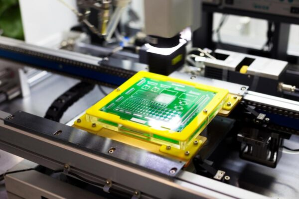
BGA (Ball Grid Array) welding is a key technology in the field of electronic manufacturing, widely used in the production and maintenance of various electronic products, such as computer motherboards, mobile phones, game consoles and so on. Because the pins of the BGA chip are distributed at the bottom of the chip in a spherical array, the welding difficulty is relatively high, and specific steps and operating guidelines need to be strictly followed to ensure the welding quality.
1、 Preparation work
Working environment: BGA soldering should be carried out in a clean, dust-free, and constant temperature environment. It is recommended to maintain a temperature of 20 ℃ -25 ℃ and a humidity of around 40% -60%. The work area should be regularly cleaned and maintained to prevent dust, impurities, and other factors from affecting the welding quality
Tool preparation:
Welding station: such as BGA repair station, can accurately control temperature and heating time, providing a stable working platform for welding.
Tweezers: Select fine and pointed tweezers for easy gripping of small components such as BGA chips and solder balls.
Soldering iron: an electric soldering iron with adjustable power and temperature, used for local heating and repair welding.
Suction nozzle: used to suck up excess solder or to suck up BGA chips during disassembly.
Hot air gun: can generate concentrated hot air, quickly heating BGA chips and surrounding areas, melting solder.
Steel mesh: Select the appropriate steel mesh based on the pin spacing and size of BGA chips for printing solder paste.
Flux, cleaning agents and other materials: Flux can enhance the activity and wettability of solder, which is helpful for soldering; Cleaning agents are used to remove impurities and residual flux after welding.
Material preparation: Prepare high-quality BGA chips, solder balls, solder paste, etc. Ensure that the BGA chip is not damaged and the pins are not oxidized; The size of the solder ball is uniform and without deformation; The composition and properties of solder paste meet the welding requirements.

2、 Processing chip
Dismantling the original chip: Use tools such as BGA rework table or large hot air duct to remove the original BGA chip from the PCB board. Attention should be paid to temperature and wind speed control during operation to avoid damage to the PCB board. Gently pick up the chip with tweezers, and while the solder joints have not cooled down, use an electric soldering iron to level and clean the solder pads on the BGA on the PCB board
Cleaning solder pads: Use tweezers to pick up a cotton ball dipped in a small amount of shampoo or specialized cleaning agent, gently wipe the BGA solder pads, remove impurities such as oxides, oil stains, and residual solder on the surface, and ensure that the solder pad surface is clean and shiny.
Dismantling the original chip: Use tools such as BGA rework table or large hot air duct to remove the original BGA chip from the PCB board. Attention should be paid to temperature and wind speed control during operation to avoid damage to the PCB board. Gently pick up the chip with tweezers, and while the solder joints have not cooled down, use an electric soldering iron to level and clean the solder pads on the BGA on the PCB board
Cleaning solder pads: Use tweezers to pick up a cotton ball dipped in a small amount of shampoo or specialized cleaning agent, gently wipe the BGA solder pads, remove impurities such as oxides, oil stains, and residual solder on the surface, and ensure that the solder pad surface is clean and shiny.
3、 Ball planting operation
Prepare steel mesh: Select the appropriate steel mesh based on the pin spacing and size of the BGA chip, and accurately place it above the BGA chip, aligning it perfectly with the pin position of the chip
Printing solder paste: Use a scraper to evenly apply an appropriate amount of solder paste onto the steel mesh
Place solder balls: Spread an appropriate amount of solder balls evenly on the BGA chip solder pads printed with solder paste
Prepare steel mesh: Select the appropriate steel mesh based on the pin spacing and size of the BGA chip, and accurately place it above the BGA chip, aligning it perfectly with the pin position of the chip
Printing solder paste: Use a scraper to evenly apply an appropriate amount of solder paste onto the steel mesh
Place solder balls: Spread an appropriate amount of solder balls evenly on the BGA chip solder pads printed with solder paste
4、 Chip mounting
Coating solder paste: Apply a thin layer of solder paste on the BGA pads of the PCB board, taking care not to apply too much solder paste, but to apply it evenly,
Chip alignment: Align the starting point (1st pin) of the BGA chip with the starting point (1st pin) of the PCB solder pad, and place the entire BGA chip inside or aligned with the silk screen frame to ensure that the chip and solder pad are perfectly aligned
Fixed chip: Place the PCB board aligned with the BGA chip and move it to the BGA repair table to fix it in place, preventing the chip from moving during the soldering process
Coating solder paste: Apply a thin layer of solder paste on the BGA pads of the PCB board, taking care not to apply too much solder paste, but to apply it evenly,
Chip alignment: Align the starting point (1st pin) of the BGA chip with the starting point (1st pin) of the PCB solder pad, and place the entire BGA chip inside or aligned with the silk screen frame to ensure that the chip and solder pad are perfectly aligned
Fixed chip: Place the PCB board aligned with the BGA chip and move it to the BGA repair table to fix it in place, preventing the chip from moving during the soldering process
RF circuit board and PCB layout characteristics
How to do PCB design
Related Article